EMI Shielding Methods for Flex PCB Designs
- Flex Plus Tech team

- Nov 17, 2025
- 4 min read
Electromagnetic interference (EMI) has become a familiar challenge in flexible PCB design—especially as devices get thinner, faster, and more compact. There’s no single “best” way to block EMI, but several practical shielding approaches have proven reliable across consumer electronics, automotive, medical, and aerospace applications.
Among all available choices, three EMI shielding methods stand out as the most widely used and most flexible-friendly:copper layers, shielding films, and silver epoxy ink. The following sections walk through what each method offers, how they behave in real flex-circuit applications, and where engineers usually apply them.
1. Copper Layers
The Classic, High-Performance Shield
Copper is always the first method designers think of. It offers the strongest shielding and is compatible with almost any high-speed or RF application.
Why it's effective
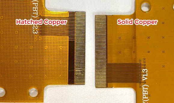
Copper has excellent electrical conductivity, so it reflects and absorbs EMI efficiently. In flexible PCBs, it can appear as:
A full copper layer dedicated for shielding (best choise)
Copper mesh for lighter weight
A copper foil laminated onto the outer surface

Where engineers use it
High-speed flex sections
FPCs carrying sensitive analog or RF signals
Automotive and aerospace modules that require guaranteed EMC performance
What to keep in mind
Copper shielding improves performance, but it also increases material cost, stiffness, and stack-up thickness—so it's commonly used when EMI performance is the top priority.
2. Shielding Film
The Most Popular Choice for Thin Flex Designs
Shielding film has become the default shielding option for many consumer electronics because it’s thin, flexible, and relatively cost-efficient.
A typical film structure includes:
A layer of aluminum or copper
Conductive adhesive
A PET or PI outer layer
Why people choose it
Very thin, ideal for ultra-slim flex cables
Good flexibility even during repeated bending
Lower weight and cost compared with full copper layers
Easy to laminate during flex PCB manufacturing
Common applications
Mobile devices and foldable electronics
Wearables
Camera modules
Display interconnects
Shielding film doesn’t provide the “absolute best” EMI performance like solid copper, but for most consumer-grade electronics, it delivers more than enough protection with much better mechanical flexibility.
3. Silver Epoxy Ink
Lightweight and Bend-Friendly
Silver epoxy ink (conductive ink) is another flexible-friendly shielding option. Instead of using a metal sheet, a thin layer of conductive ink is printed on the flex surface or coverlay.

Why engineers like it
Extremely thin and lightweight
Very high flexibility — good for dynamic-flex designs
Suitable for large-area shielding without adding much stiffness
Cost-effective compared with metal layers
Things to consider
Not as strong as copper in terms of EMI performance
Must be printed with stable process control to avoid cracks
Best for low-to-medium EMI environments
Where it's commonly used
Smart wearable bands
Soft medical devices
Consumer devices with lightweight flex circuits
Low-voltage interconnects
Silver ink gives a balanced combination of low cost, bendability, and easy application.

Other EMI Shielding Options
While the three methods above cover most flexible PCB needs, other approaches still appear in certain applications. These are usually supplementary or used together with the main methods:
Grounded guard traces / ground pour
Simple, effective, and commonly used to reduce noise coupling around sensitive lines.
Metalized coverlay
A PI film coated with metal — good for flexible but rugged designs.
Shielding cans in rigid-flex circuits
Used when the rigid section carries RF modules or antennas.
Conductive tapes
Handy for prototyping or simple EMC fixes but rarely used as a long-term production solution.
These methods help, but they are usually not the primary shielding strategy for modern flexible PCB boards.
EMI Shielding Methods Comparison
Shielding Method | Pros | Cons |
Copper Layers | • Most effective shielding method • Controlled-impedance capable • Best for high-density component areas • Suitable for all flex and rigid-flex PCB designs • Can be extended under stiffeners | • Higher cost and reduced flexibility • Significant flex-thickness increase • Mesh copper improves bendability but reduces shielding • Added process steps and materials increase cost • Limited use on >2-layer flex circuits due to bend requirements • Takes additional circuit area (extra vias for SMT grounding) |
Shielding Film | • Very effective shielding—close to copper • Most cost-effective and flexible solution • Can be used in component areas with some limits • Suitable for both flex and rigid-flex • Most used method for non-impedance-controlled designs • Wide variety of films available | • Not recommended for controlled-impedance designs • Larger impedance tolerance and dielectric-thickness variation • Limited in high-density component areas (film thickness constraints) • Exposed ground circuit at flex outline • Stiffeners cannot be laminated directly (friction-resistant surface) • Requires PSA for stiffener attachment |
Silver Ink | • Effective EMI shielding • Lower cost than copper • More flexible than copper shield layers • Can be extended under stiffeners • Can be used (with limits) on higher-layer flex designs • Long-established method used for decades | • Many additional process steps (1-2 print + bake cycles) • Requires 1-2 extra coverlay layers • Reduced bend capability due to added thickness • Not recommended for controlled-impedance circuits • Difficult to achieve required dielectric thickness • Not compatible with rigid-flex PCB structures • Very limited for high-density areas. |
Conclusion
Flex PCB EMI shielding doesn’t rely on one universal solution. Copper layers, shielding film, and silver epoxy ink each offer different benefits — whether you need top-tier EMC performance, ultra-thin construction, or excellent bend reliability.
Learn more about flexible PCBs, from key design considerations to full fabrication processes.


Comments