Pad Design Guidelines for Flexible PCB Components
- Flex Plus Tech team

- 4 hours ago
- 4 min read
Flexible printed circuits are widely used in compact electronic systems where mechanical flexibility and space savings are required. However, component pad design on flexible PCBs presents unique challenges that are rarely encountered in rigid boards.
Engineers often experience issues such as cracked solder joints, pad lifting, or copper fatigue when components are mounted on flexible circuits. In most cases, these failures are not caused by materials or assembly defects, but by improper pad design in areas subject to bending or mechanical stress.
This article explains practical pad design guidelines for flexible PCB components, focusing on engineering solutions that improve solder joint reliability and mechanical durability.
Mechanical Stress Is the Primary Design Constraint
Unlike rigid PCBs, flexible circuits are designed to bend, fold, or dynamically move during product operation. When a flex circuit bends, different layers experience different levels of mechanical stress:
Copper traces undergo tensile and compressive stress
Solder joints experience cyclic fatigue
Pads may delaminate from the polyimide substrate
If component pads are located in bending zones, the solder joints become mechanical load points, which can eventually cause failure.
For this reason, pad design must focus on stress reduction and stress distribution rather than simply electrical connectivity.
Component Placement Strategy
The most effective solution is avoiding component placement in dynamic flex regions.
Recommended placement zones include:
Stiffened areas
Rigid sections of rigid-flex circuits
Static regions that do not bend during operation
When components must be placed near a bending zone, the designer should increase the distance between the component pads and the bend line.
Typical engineering practice:
Minimum distance from component pad to bend line: 2–3× the flex thickness
This prevents solder joints from becoming the primary stress points during bending.
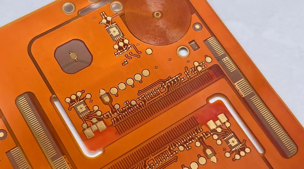
Teardrop Pad Transition to Prevent Trace Cracking
A common failure point in flexible circuits occurs at the junction between the trace and the pad.
Standard pad-to-trace connections create a sharp transition that concentrates mechanical stress. During repeated bending cycles, copper can crack at this location.
To mitigate this problem, designers typically use teardrop pad structures.
Advantages of teardrop transitions include:
Smoother stress distribution
Reduced copper fatigue
Stronger mechanical anchoring of traces to pads
Teardrops are particularly recommended for: small SMT pads,fine-pitch components and circuits exposed to repeated flexing
Reinforcing Component Pads with Stiffeners
For most SMT components mounted on flexible PCBs, stiffeners are essential.
Stiffeners provide a rigid base that stabilizes the pad area during soldering and operation.
Common stiffener materials include:
FR-4 stiffeners for standard electronic assemblies
Polyimide stiffeners for fully flexible constructions
Stainless steel stiffeners for high-strength applications
Without stiffeners, pads may experience:
Uneven solder joints
Pad lifting during reflow
Deformation of the flex substrate
In engineering practice, stiffeners are usually placed directly beneath the component mounting area to ensure planarity and mechanical stability.
Optimizing Pad Geometry for Flexible Substrates
Pad geometry that works well on rigid boards may not perform reliably on flexible substrates.
Recommended pad design improvements include:
1. Rounded pad corners
Sharp corners increase stress concentration in copper layers. Rounded edges help distribute mechanical stress more evenly.
2. Slightly enlarged pad dimensions
Pads on flexible circuits are often designed slightly larger than standard IPC recommendations to improve solder joint strength.
3. Balanced copper distribution
Uneven copper around component pads can cause localized stiffness variations, which increases the risk of pad fatigue.
Balanced copper helps maintain consistent mechanical behavior across the flex area.

Coverlay Opening Design Around Flexible PCB Pads
Flexible PCBs typically use coverlay instead of solder mask. The size and shape of the coverlay opening can significantly affect pad reliability.
Key considerations include:
Sufficient clearance between pad edge and coverlay opening
Smooth coverlay edges to prevent stress concentration
Proper adhesive bonding around pad areas
If the coverlay opening is too small, adhesive stress may concentrate around the pad edges and increase the risk of pad lifting.
Managing Pads Near Bend Areas
In some flexible PCB designs, pads must be located close to flexing areas due to space constraints. In such cases, additional engineering strategies can be applied.
Possible solutions include:
Increasing copper thickness in the pad region
Reinforcing the pad area with additional polyimide layers
Relocating the bend line slightly away from the component pads
Using staggered pad layouts to distribute stress
These approaches reduce mechanical strain on the solder joints and improve long-term durability.
Surface Finish Considerations
Pad surface finish also influences solder joint performance in flexible PCB assemblies.
Common finishes include: ENIG,Immersion Gold,OSP
For flexible circuits used in high-reliability applications, ENIG is often preferred because it provides consistent pad flatness and excellent solderability.
Stable surface finishes help ensure uniform solder joints, which improves mechanical strength in dynamic environments.
Typical Failure Modes Caused by Poor Pad Design
When pad design does not account for flex mechanics, several common failures can occur:
Solder joint cracking after repeated bending
Pad lifting from the substrate
Copper trace fractures near pad connections
Intermittent electrical connections
Most of these problems can be prevented by implementing proper pad geometry, stiffener reinforcement, and component placement strategies.
Conclusion
Pad design for flexible PCB components requires a different engineering approach than rigid PCB layouts. Designers must consider mechanical stress, bending behavior, and substrate flexibility when defining pad structures.
By applying optimized pad geometry, teardrop transitions, stiffener reinforcement, and proper component placement strategies, engineers can significantly improve the reliability of flexible PCB assemblies in real-world applications.
These design practices help ensure stable solder joints and long-term durability, even in products that experience continuous bending or movement.


Comments