

How to Control Copper Balance in Multilayer Flex PCB Production

Copper balance is one of the key factors affecting the quality and reliability of multilayer flex PCB production. An uneven copper distribution between layers can cause problems such as board warpage, dimensional instability, uneven etching, and difficulties during lamination.
Unlike rigid PCB, multilayer flexible circuits use thin dielectric materials and copper foils, making them more sensitive to mechanical stress. Proper copper balance design and manufacturing control are essential to achieve stable production results.
In this article, we will discuss why copper balance matters in multilayer flex PCB manufacturing and how PCB manufacturers control it during design, fabrication, and mass production.
What Is Copper Balance in Multilayer Flex PCB?
Copper balance refers to the uniform distribution of copper areas across different layers of a multilayer flex PCB.
During FPC manufacturing, each copper layer creates mechanical stress because copper and dielectric materials have different coefficients of thermal expansion (CTE). When one side contains significantly more copper than the other side, the internal stress becomes uneven after lamination and curing.
For example, if the outer layer has large copper areas while the opposite layer has very little copper, the flex PCB may bend or twist after the lamination process.
A well-balanced copper structure helps maintain:
Stable PCB thickness
Better dimensional accuracy
Reduced warpage
More consistent etching results
Improved yield during production
Why Copper Balance Is Important for Multilayer Flex PCB Manufacturing
Preventing Flex PCB Warpage
Warpage is one of the most common issues caused by poor copper balance.
During the multi-layer lamination process, heat and pressure are applied to bond copper layers, coverlay, and adhesive materials together. Different copper densities create uneven stress when the PCB cools down.
In multilayer FPC production, this problem can become more serious because the overall thickness is usually very small. Even a small amount of stress can affect assembly performance.
A balanced copper distribution reduces internal stress and helps the finished flexible circuit maintain its designed shape.
Improving Dimensional Stability
Multilayer flex PCB requires high dimensional accuracy, especially for applications such as display modules, medical devices, cameras, and precision electronic products.
Uneven copper distribution can cause local expansion or shrinkage during:
Lamination
Plasma treatment
Surface finishing
Thermal processes
Maintaining copper balance helps control layer-to-layer registration and improves the accuracy of drilling, laser processing, and assembly.

How Manufacturers Control Copper Balance in Flex PCB Production
1. Optimizing Layer Stackup Design
Copper balance starts from the PCB design stage.
When designing a multilayer flex PCB stackup, engineers should consider the copper distribution of each layer instead of focusing only on electrical routing.
For example, if one signal layer contains large copper areas while the opposite layer has mostly empty space, designers may add copper balancing areas to reduce the difference.
However, copper balancing areas should not affect impedance requirements, signal performance, or flexible bending areas.
At Flex Plus, we usually review copper distribution during the engineering review stage before production to identify potential stress problems early.
2. Adding Copper Fill Areas
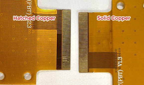
One common method to improve copper balance is adding copper fill areas in unused regions.
Copper fills can be designed as:
Solid copper areas
Copper grids
Hatched copper patterns
For flexible circuits, copper grids or hatched copper are often preferred because they provide stress control while maintaining flexibility.
The copper fill design needs to consider:
Bending requirements
Signal interference
Manufacturing capability
Minimum copper spacing rules
Adding too much copper is not always better. Excessive copper may increase stiffness and reduce the flexibility of the FPCB.
3. Controlling Copper Density During Etching
Copper balance is also affected by the manufacturing process.
During the etching process, areas with different copper densities may experience different etching rates. Large isolated copper areas and dense circuit areas can result in uneven line width after etching.
Manufacturers need to control:
Etching parameters
Copper pattern distribution
Line compensation
Etching solution condition
For multilayer flex PCB, maintaining stable etching performance is important for achieving consistent fine-line circuits.
4. Balancing Copper on Symmetrical Layers
For multi-layer flexible circuits, symmetrical layer structures usually provide better mechanical stability.
For example, a 4-layer FPC with similar copper distribution between the top and bottom layers will generally have less stress compared with an unbalanced structure.
However, perfect symmetry is not always possible because different layers may have different electrical functions. In these cases, engineers need to find a practical balance between electrical requirements and mechanical reliability.
5. Considering Copper Balance During Lamination
The lamination process is where copper balance problems often become visible.
Important lamination factors include:
Temperature profile
Pressing pressure
Adhesive flow
Material thickness
Heating and cooling rates
Even with a good design, improper lamination parameters can still cause deformation.
Experienced flexible circuit manufacturers usually verify the stackup design together with lamination parameters to achieve consistent results.
Common Copper Balance Problems in Multilayer Flexible PCB Production
Excessive Copper Difference Between Layers
When one layer contains significantly more copper than another, the finished FPC may show:
Curling
Twisting
Local bending
Poor assembly alignment
Copper Balance Ignored in Large Flexible Circuits
Large-area flexible PCBs are more sensitive to copper imbalance because the accumulated stress becomes greater over a larger area.
For long FPC cables or large flexible circuits, copper distribution should be carefully reviewed before tooling.
Adding Copper Without Considering Flexibility
Copper balancing should not reduce the bending performance of the flexible PCB.
In dynamic bending applications, copper fill design must avoid stiffening the bending area.
Design Recommendations for Better Copper Balance
To improve copper balance in multilayer flex PCB production, designers should:
Use similar copper coverage between symmetrical layers when possible.
Avoid large empty copper areas on one side of the stackup.
Use copper balancing patterns in non-critical areas.
Consider bending zones separately from static areas.
Discuss copper distribution with the flexible PCB manufacturer before mass production.
Conclusion
Copper balance plays an important role in multilayer flex PCB production. Proper control of copper distribution helps prevent warpage, improve dimensional stability, and increase manufacturing yield.
Because flexible circuits use thin materials and require precise mechanical performance, copper balance should be considered from the initial PCB design stage through lamination and final inspection.
An experienced FPC manufacturer can help optimize copper distribution based on the application, layer structure, and production requirements, ensuring reliable performance in real-world products.


Comments