

How Are Flexible PCBs Shielded for EMI and RFI Protection?

Flexible PCBs are already widely used. Their thin and flexible structure makes them easy to install in small spaces, but it also presents challenges in protecting against electromagnetic interference and radio frequency interference.
So, how are flexible PCBs shielded for EMI and RFI protection?
The answer usually involves copper, conductive ink, or specialized shielding films. However, the shielding material is only part of the solution. Grounding, stack-up design, and bending requirements are equally important.
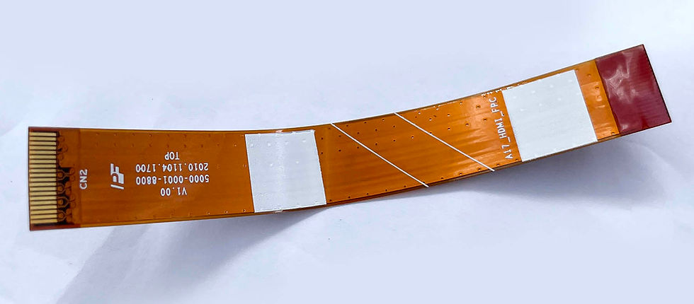
Common Flexible PCB EMI Shielding Methods
Copper Shielding
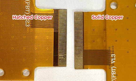
It can be added as a dedicated ground or shielding layer in the flexible circuit board stack-up. Because copper has high electrical conductivity, it provides an effective path for unwanted electromagnetic currents.
Copper shielding works well for high-speed circuits and areas requiring stronger EMI protection. But, thicker copper can increase the stiffness of the flexible PCB. It may therefore be less suitable for areas that require frequent dynamic bending.
Conductive Silver Ink
It can be printed over the flexible circuit to create a thin shielding layer. It’s useful when low thickness and good flexibility are important.
However, its resistance is usually higher than that of bulk copper, so we should consider the required shielding performance and application frequency before choosing this method.
EMI Shielding Film
Specialized EMI shielding films are widely used in compact flex PCB applications. They typically combine a conductive layer with an insulating layer and conductive adhesive.
The main advantage is the balance between EMI protection, thin, and flexibility. This makes shielding film suitable for wearable devices, cameras, smartphones, and other applications with limited space.
Grounding Is Critical
Adding a conductive shield does not automatically provide effective EMI protection.
The shielding layer needs a reliable connection to ground. Poor grounding or discontinuities in the shielding structure can reduce its effectiveness.
For this reason, manufacturers need to consider:
Ground connection points
Shield continuity
Conductive adhesive
Ground-plane structure
Openings around sensitive areas
In many cases, a well-grounded smaller shield can perform better than a larger shield with a poor return path.
Shielding Must Not Compromise Flexibility
One of the biggest differences between rigid PCBs and flexible PCBs is mechanical movement.
A shielding layer adds material to the flexible PCB structure. If the shield is too thick or too rigid, repeated bending may increase mechanical stress and eventually cause cracking, delamination, or loss of electrical continuity.
Therefore, dynamic bending areas may require thinner shielding structures, while static areas can use more robust shielding.
This is why EMI shielding for flexible PCBs should be designed together with the bending requirements, rather than added after the flexible PCB layout is finished.

EMI Shielding and Impedance Should Be Considered Together
For high-speed flexible circuits, the shielding layer also affects signal impedance.
The distances between signal traces, dielectric layers, and ground or shielding layers can alter the electrical characteristics of a circuit.
Therefore, when designing a layer stack-up, trace width, dielectric layer thickness, copper layer thickness, and shielding layer placement must be comprehensively considered.
Adding a shielding layer only in the final design stage may require adjustments to the signal structure.
The Key to Reliable Flexible PCB Shielding
The goal is not simply to create the strongest possible shield.
A good flexible PCB EMI shielding solution needs to balance:
EMI/RFI protection + grounding + signal integrity + flexibility + manufacturing reliability
Copper foil, conductive ink, and shielding films can all provide shielding. The choice of shielding material depends on the desired shielding performance, frequency range, bending conditions, thickness limitations, and the overall structure of the PCB.
For flexible PCB applications, the optimal shielding solution typically provides sufficient electromagnetic protection while maintaining flexibility or long-term reliability.


Comments