Flex PCB Solder Defects: Twist, Bending, and Weld Leg
- Flex Plus Tech team

- Dec 1, 2025
- 2 min read
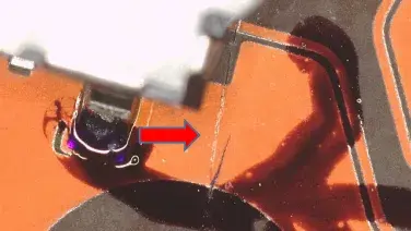
Flex PCB solder defects are common in flexible circuits because the boards bend, twist, and warp more easily than rigid PCBs. These deformations can cause uneven soldering, misaligned components, and weak joints. The main causes are twist and bending of the flexible PCB and weld-leg (pin leg) issues. Understanding these factors is key to reliable assembly.

Twist and Bending
Flexible PCBs are thin and soft, so small movements during handling, printing, or reflow can cause twist or bending. Even minor deformations can create problems:
Pads may sit at different heights
Component pin legs may not sit flat on solder paste
Solder joints can have uneven thickness, leading to open or cold joints
Optical components like LEDs or sensors can tilt
How to minimize twist and bending effects:
Use rigid carriers, stiffeners, or vacuum plates to keep the board flat
Check and maintain flatness before placement (<0.2 mm warpage)
Avoid rapid temperature changes during reflow
Support ultra-thin flexible PCBs with panel frames or edge rails
Twist and bending often lead to weld-leg problems in component placement.
Weld Leg — Pin Behavior on Uneven Surfaces
A weld leg is the metal terminal or pin that contacts solder paste. On a warped or uneven FPCB, different pin legs land at different heights, which can cause:
High-sitting legs → no solder → open circuit
Low-sitting legs → excess solder → bridging
Components rocking during reflow → skew or tombstoning
Fine-pitch ICs particularly sensitive to uneven pin placement
Preventing weld-leg defects:
Keep the flexible PCB board flat during stencil printing and placement
Check coplanarity of pin legs for sensitive components
Adjust stencil paste distribution for outer pads
Maintain uniform adhesive thickness in COB assembly
Factor | Risk if Ignored | Mitigation |
Twist & Bending | Uneven pad contact, open joints, component tilt | Flat support, stiffeners, careful handling, controlled reflow |
Weld Leg / Pin Leg | Open joints, bridging, skew, tombstoning | Coplanarity checks, stencil paste adjustment, adhesive height control |
Common Flex PCB Solder Defects
Typical defects resulting from twist, bending, and weld-leg issues include:
Pad lifting — pads detach from the PI substrate due to stress
Cold solder joints — poor wetting from uneven paste or rapid cooling
Solder bridging — caused by uneven pad heights
Component shifting — soft FPC allows movement during reflow
Cracked solder joints — bending during assembly or in-field use
Tips to Reduce Solder Defects
Design and Layout:
Avoid placing solder joints in high-bending areas
Add stiffeners under heavy or sensitive components
Use reasonable pad sizes to reduce lifting
Handling and Placement:
Keep flexible circuits flat during transport and assembly
Use trays, plates, or support structures to stabilize boards
Optimize solder paste printing and volume
Reflow and Assembly:
Adjust reflow profiles for PI and copper stack-ups
Ensure components are properly aligned and coplanar
Monitor soldering quality and perform bend-cycle or pull tests as needed

Summary
Mechanical stability is critical for flex PCB solder quality. Controlling twist, bending, and weld-leg behavior ensures consistent solder joints, reduces rework, and improves long-term reliability for SMT and COB assemblies.


Comments